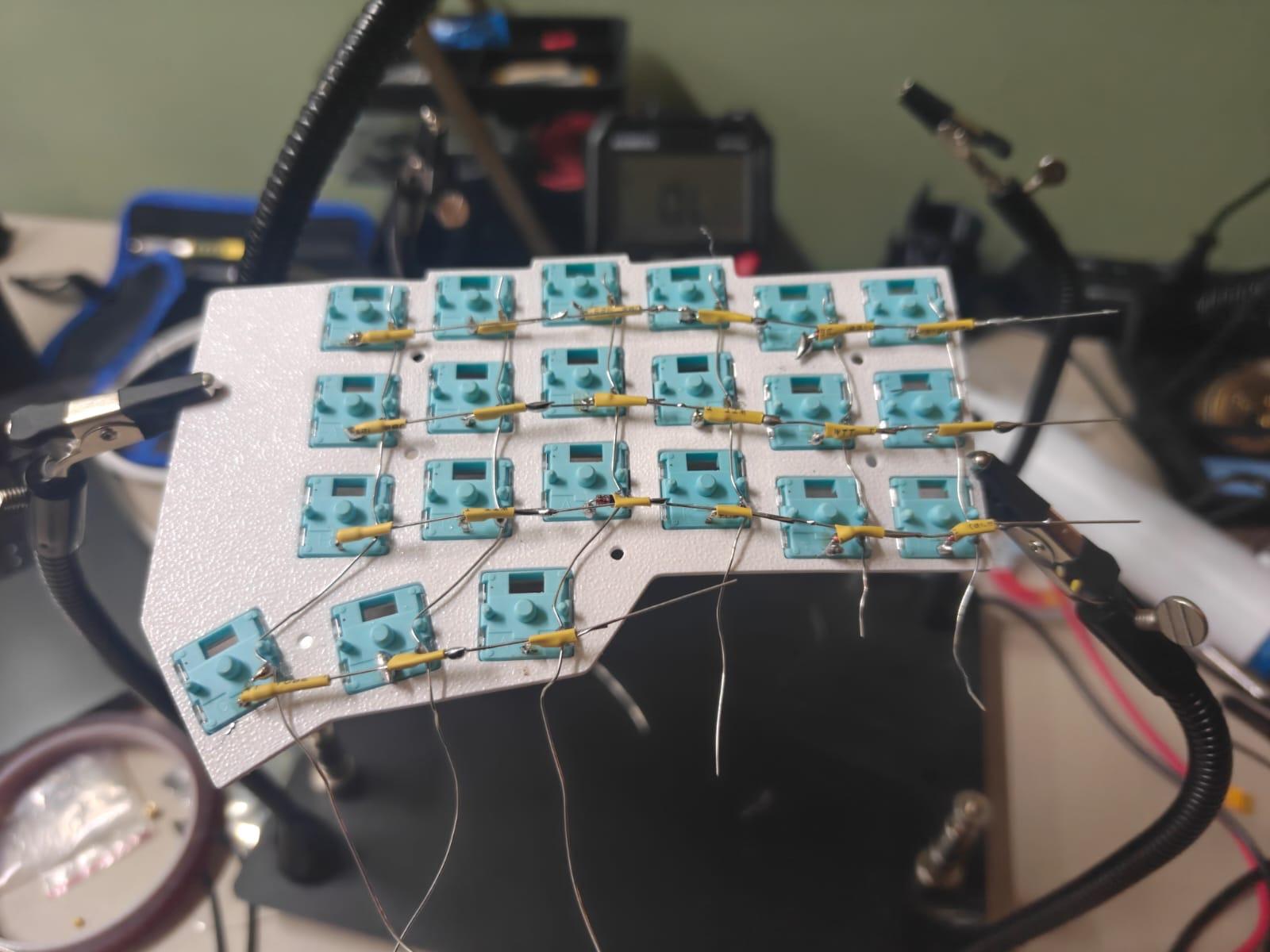
Part 1 of a series. Later parts cover the case, the right half and the final build.
This is not a guide yet. It is a log of my first attempt, with the mistakes left in. I will write a proper step-by-step guide when the final version works.
Where things stand after day one:
- The left half works. All 21 keys type over USB, running ZMK firmware.
- Three case designs failed or are still untested.
- The next idea is to put the controller board on top of the plate instead of hiding it inside the case.
Why build one at all
I type all day. A split keyboard lets each hand sit in its own natural spot, so my shoulders stay open. Wireless means no cable between the halves and none to the laptop.
You can buy one. But building it teaches you how a keyboard actually works. I wanted to know what happens between pressing a key and a letter showing up on screen. I also wanted a reason to learn soldering properly.
The build that got me started was a YouTube video, "How to build a Corne Keyboard - Wireless, Split, Ergonomic, Cheap". It claims about 25 dollars of parts. A Corne has 21 keys on each half, so 42 in total.
The parts
I bought more than I needed, so I have spares for mistakes and a second keyboard.
| Part | Notes | Price |
|---|---|---|
| 4 Pro Micro nRF52840 boards | A cheap copy of the nice!nano. Two per keyboard. | Rs 799 each |
| 500 1N4148 diodes | One per key | |
| 5 LiPo cells, 480 mAh | One per half | |
| 15 slide switches | Power on and off | |
| 10 m of 24 AWG solid-core wire | Rows and columns | |
| YIHUA 948DB+-II soldering station | T12 tips | |
| Solder, flux, wick | ||
| M2 screws and brass inserts | To hold the plate in the case |
I already had a Bambu Lab 3D printer, PLA and PETG plastic, Kailh Choc and MX switches, and keycaps. For this build I used Choc v1 Robin switches. They are clicky, low profile, and need 47 g to press.
What I learned before touching the iron
I made two short narrated videos to teach myself the basics. They cover the two ideas the whole build rests on.
The controller board
The Pro Micro nRF52840 is a tiny computer. Its only job is to turn key presses into Bluetooth messages. The nRF52840 chip holds the processor, the memory and the Bluetooth radio. The USB-C port loads the firmware and charges the battery.
Down both edges are pins. Each pin can only answer one question: is it connected right now? A key switch is just a gap in a wire. Press it, the gap closes, and a pin sees the connection.
The controller board, explained in under two minutes
Rows, columns and diodes
A half has 21 keys but the board has far fewer usable pins. So the keys sit in a grid. Every key is where a row wire crosses a column wire. A Corne half needs 4 rows and 6 columns, so 10 pins instead of 21.
The chip turns on one row at a time, very fast, and checks which column answers. Row 1 on and column 1 answers? That must be the S key.
There is a catch. Press three keys that form a square, and current can sneak backwards through them. The board then sees a fourth key you never pressed. This is called ghosting.
A diode fixes it. It lets current flow one way only. The 1N4148 is a small glass bead with a black stripe. Current flows toward the stripe. One diode per key, all facing the same way, and the firmware has to be told which way that is.
Why every key needs a diode
Day 1 on the bench
Setting up safely
Goggles on. An air purifier next to the bench and the window open, because flux smoke is not something to breathe. I did not have a heat mat, so I used a ceramic tile. The iron was set to 320 C. I cleaned the tip in brass wool and coated it with fresh solder before starting.
The first solder joint
I practised on two pieces of scrap wire first. Solid-core wire is too stiff to twist together, so I laid the bare ends side by side.
The method: heat the copper for about two seconds. Feed solder from the other side, so the wire melts it, not the iron. Take the solder away first, then the iron.
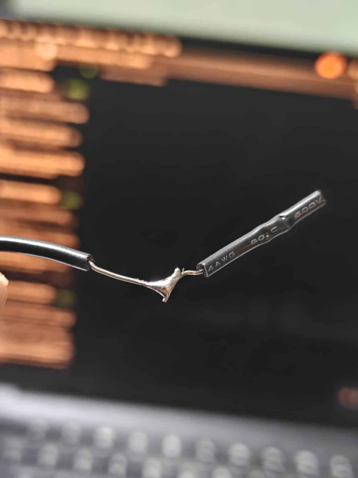 My first joint. Shiny, so not a cold joint. But I stripped too much wire on one side and left a small spike by lifting the iron slowly.
The next joint was a diode leg onto a wire. The lesson there was overlap. If the leg only touches the tip of the wire, the contact is tiny. Lay them side by side for 3 to 5 mm.
Learning the multimeter
I did not know how to use a multimeter. Three things made it click.
- Continuity mode (the sound wave symbol) beeps when two points are connected. This is the mode I used all day. Touch both ends of a joint. Beep means connected.
- Diode mode shows how a diode behaves. Red probe on the plain end, black on the stripe end, gave 0.6. That means current flows. Swap the probes and it showed OL, which means blocked. So the diode was good and facing the way I thought.
- Hold the probes properly. When I held a battery wire against a probe with my fingers, the reading jumped between 0.2 and 1.6 V. Clamped and pressed onto bare metal, it read a steady 3.x V. The battery was fine. My grip was not.
One more trap: the helping hands have metal clips, and they are all joined through the metal stand. Testing a part while it sits in the clips can give false readings. Take it out first.
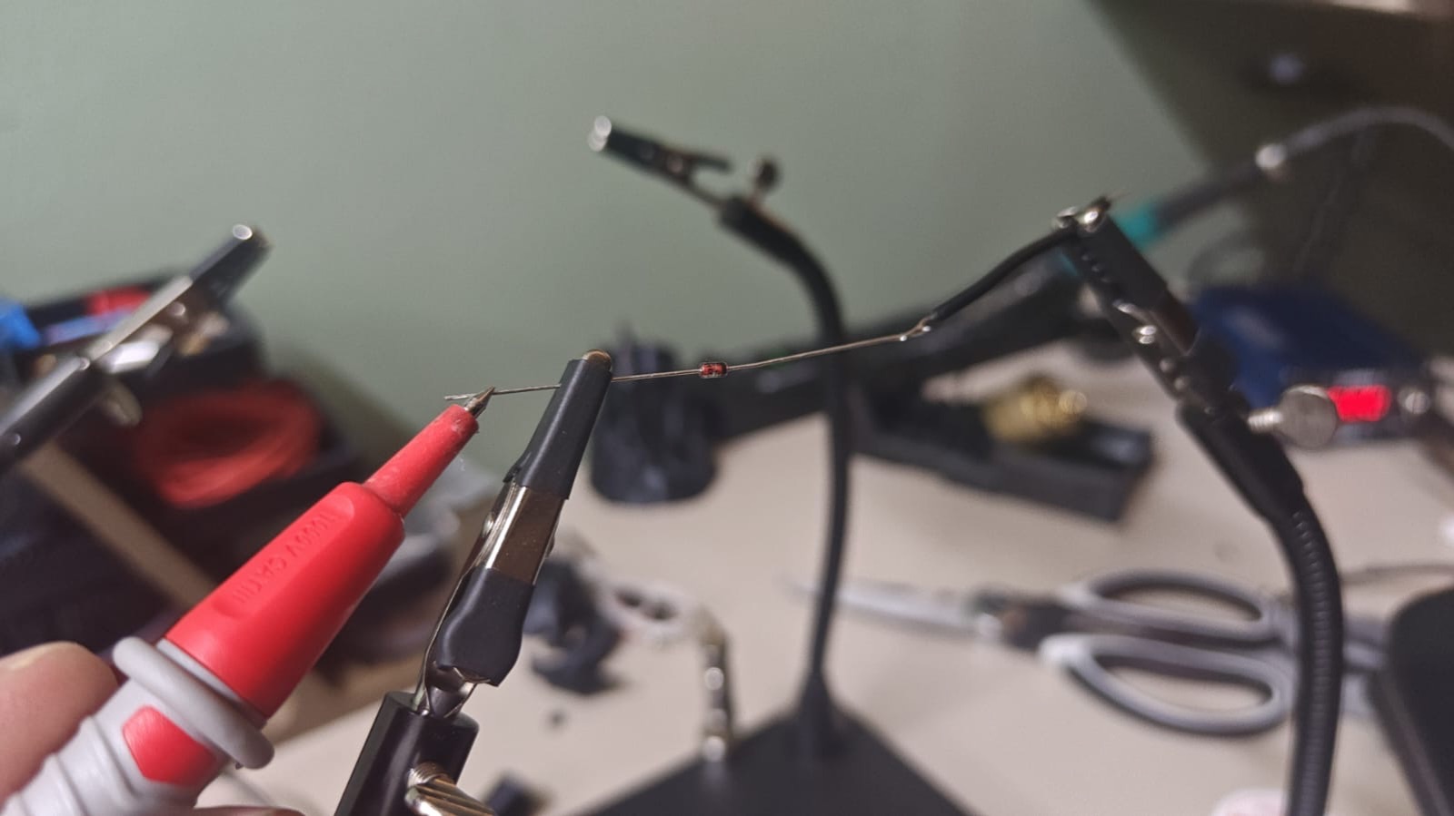 Diode mode on a diode soldered to a wire. 0.6 one way, OL the other.
A test plate first
The plate is the flat piece the switches clip into. I used the left and right case files and the plate from the video creator's GitHub repo (milar111/Corne). Before printing anything big, I printed only the plate to check the switch holes. It took 26 minutes and 8.3 g of white PLA.
The test plate finishing on the printer
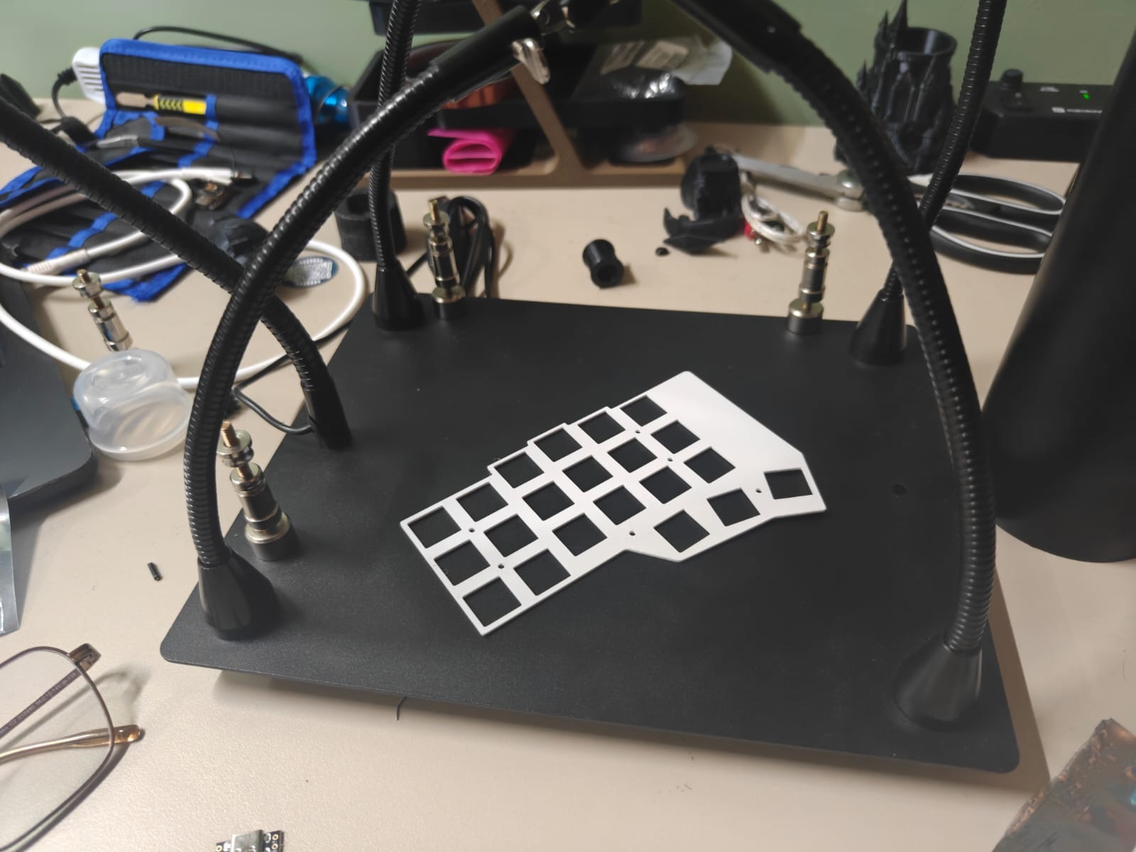 The printed test plate. Sharp square holes, 19 mm apart.
My first try at fitting switches was wrong. I pushed them in the wrong way round, so they were loose and fell out when I flipped the plate. The second try worked. All 21 sat flat and firm, all facing the same way, including the three angled thumb keys.
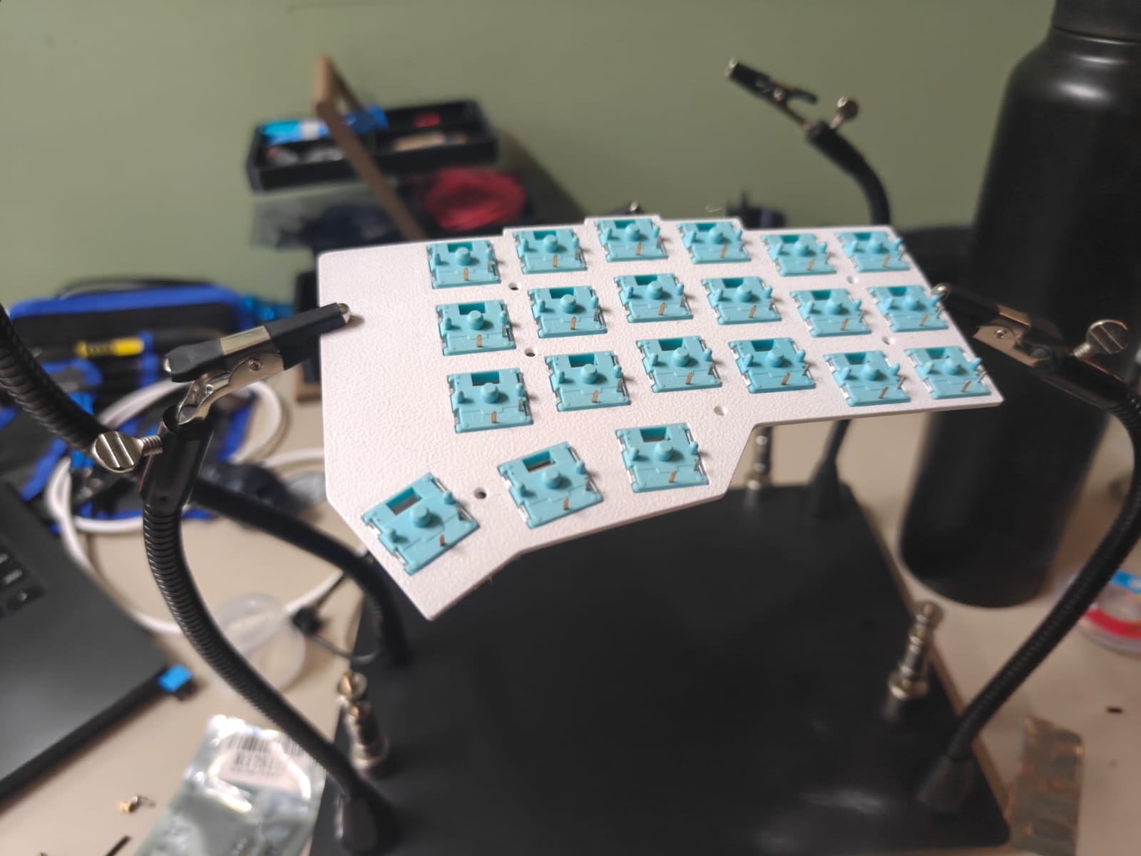 All 21 Choc Robin switches in the plate
Wiring the grid by hand
Hand-wiring means no circuit board. Every row and every column is a wire you solder yourself, straight onto the switch pins. Each switch has two pins on the back. One pin gets the diode, which leads to the row. The other pin gets the column wire.
I followed the order from Joe Scotto's video "How to Build a Handwired Keyboard": columns first, then diodes, then rows, then the board.
Columns first
For each column I took bare copper wire and bent it into a gentle wave that hooks onto each switch's column pin. The wave holds the wire in place while you solder, so you don't need a third hand.
Rules I set myself: never touch the other pin, keep the wire flat so the case still fits, and nothing past the edge of the plate. The inner three columns also reach down to a thumb key.
After each column I checked it with the multimeter. One probe stays on the end of the wire. The other touches each pin in turn. Every one should beep. Testing only end to end proves the wire is whole, not that each joint is good.
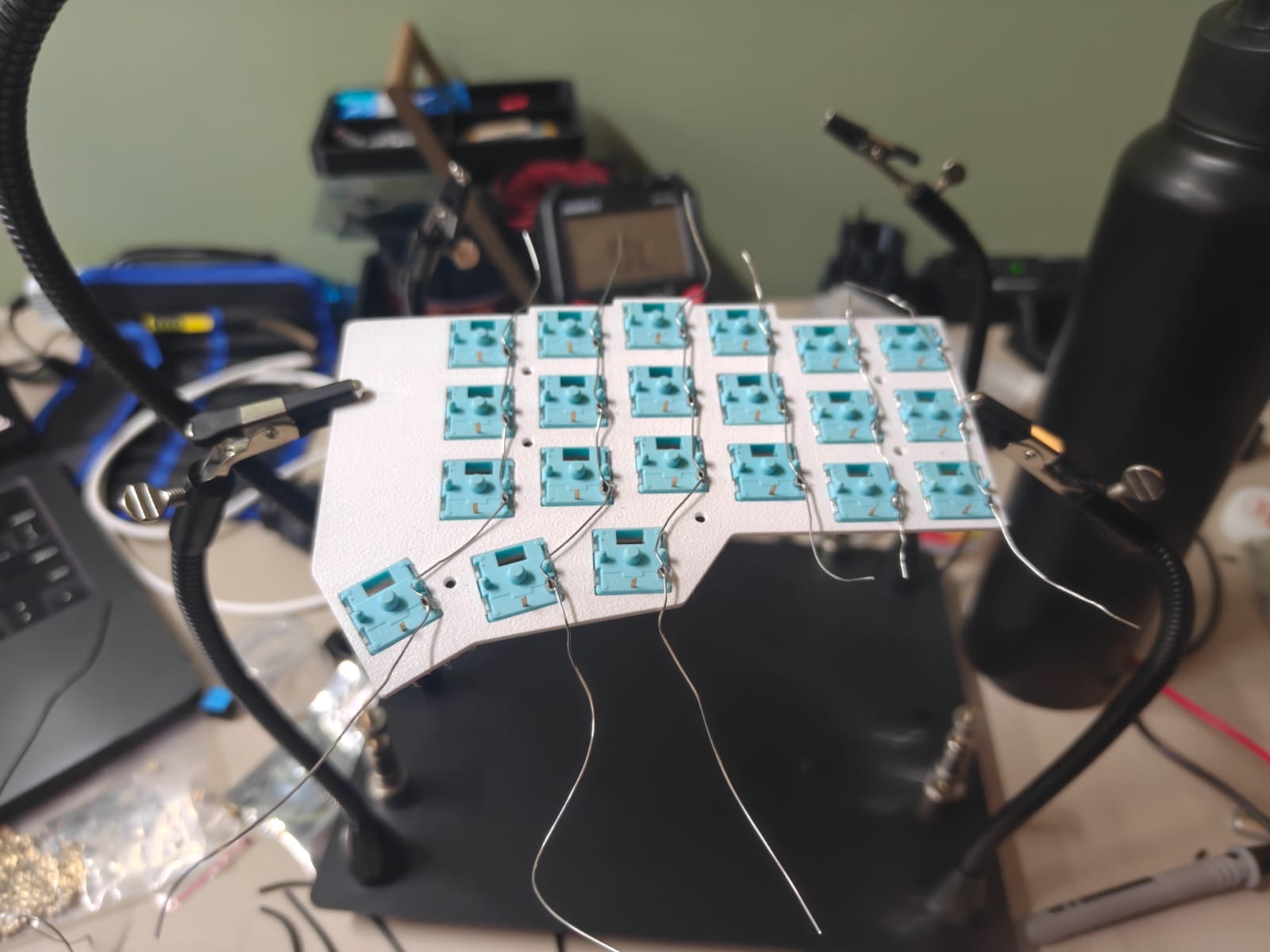 All six columns soldered. The bottom ends are left long to reach the board later.
Diodes, chained into rows
Each key gets a diode. The plain leg is trimmed short and soldered to the switch's diode pin. The stripe leg is left long. Then the long legs in a row are joined together, one to the next. The legs themselves become the row wire.
The problem is that the bare row legs cross the bare column wires. If they touch, the row and column short together and the key is broken. So every crossing needs insulation.
I changed my mind on this three times. I tried a separate insulated row wire. I thought about Kapton tape over each column. In the end I chained the diode legs and slid a small piece of heat-shrink tube over each leg where it crosses a column.
A good trick: put the leg arriving from the left and the leg going to the right into the same sleeve. The sleeve holds them tight together, which makes them easy to solder. That is fine because both legs belong to the same row. Keep the solder spot outside the sleeve, and keep the sleeve over the crossing.
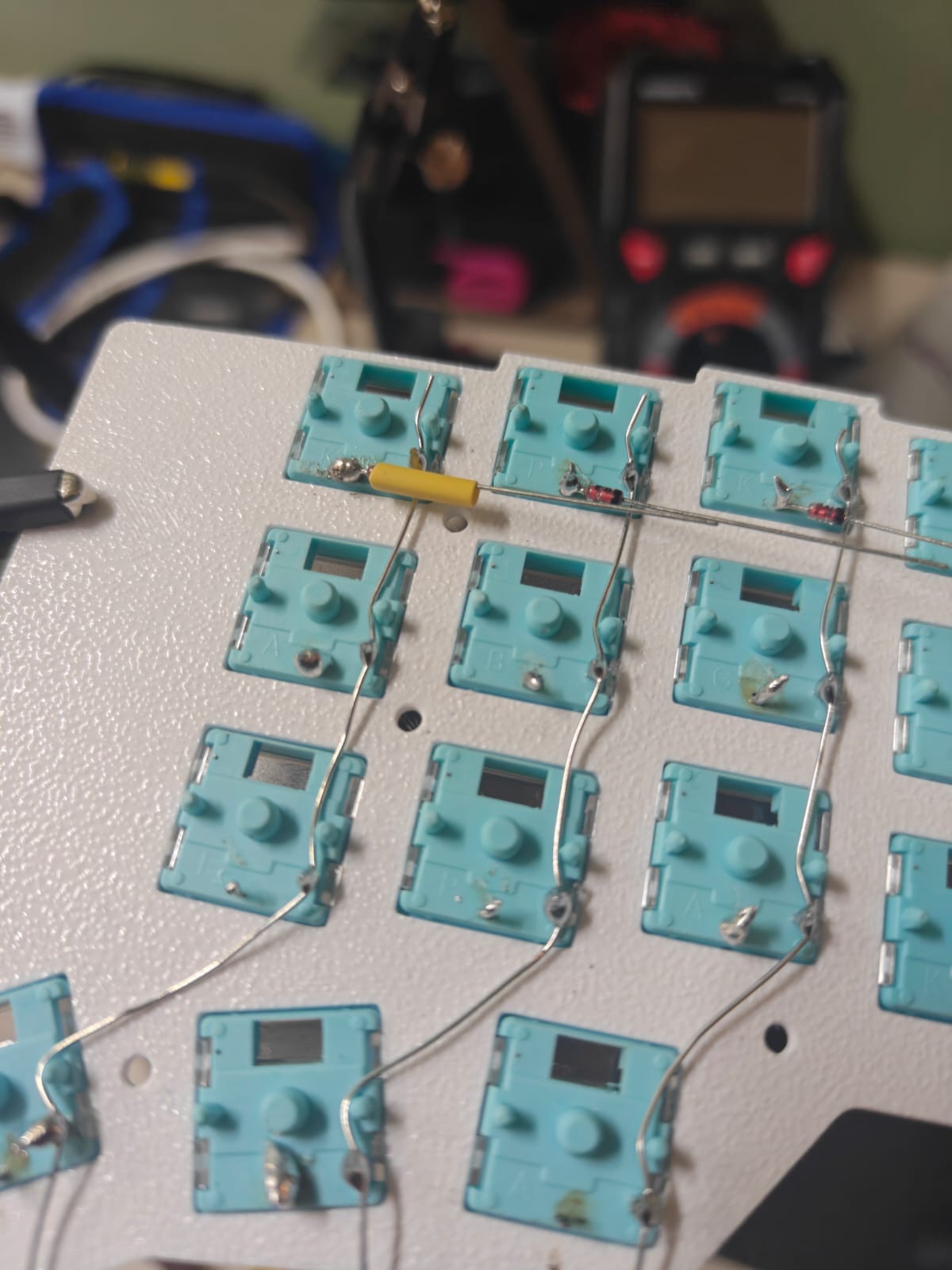 The first sleeve on the first diode leg, right where it crosses a column wire
A heat gun shrinks the tube so it grips the wire.
Shrinking the sleeves with a heat gun
After each row I ran two tests. Every joint along the row should beep. And the row tested against each column should stay silent. A beep there means a short.
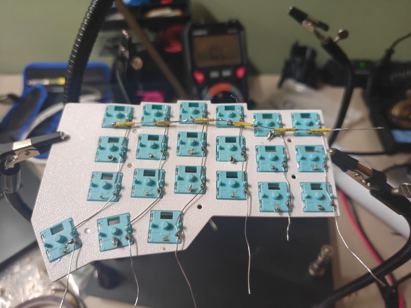 The top row done. Six diodes chained, with a yellow sleeve at every crossing.
On the second row the long legs pointed up toward the top row. I had to bend them flat and sideways along their own row, so they could not touch the row above. The thumb row was the hardest, because the wire has to follow the angled thumb keys.
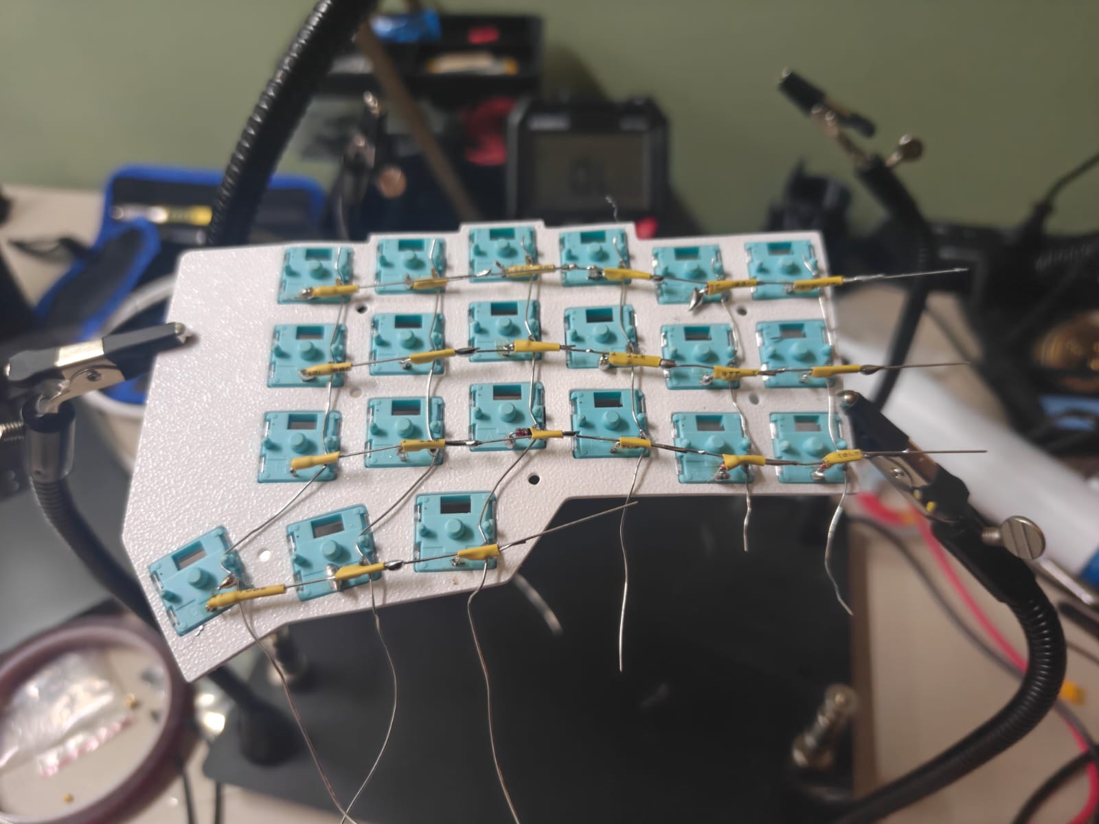 The full grid: 6 columns and 4 rows, with long ends left for the board
Connecting the board
Before wiring it in, I plugged the board in by USB. It showed up as a drive called NICENANO, so it was alive and ready for firmware.
Then I read the real pin labels off the board with a magnifier. My plan was based on a diagram, and the clone's labels did not all sit where I expected. Never trust a pin diagram over the board in your hand.
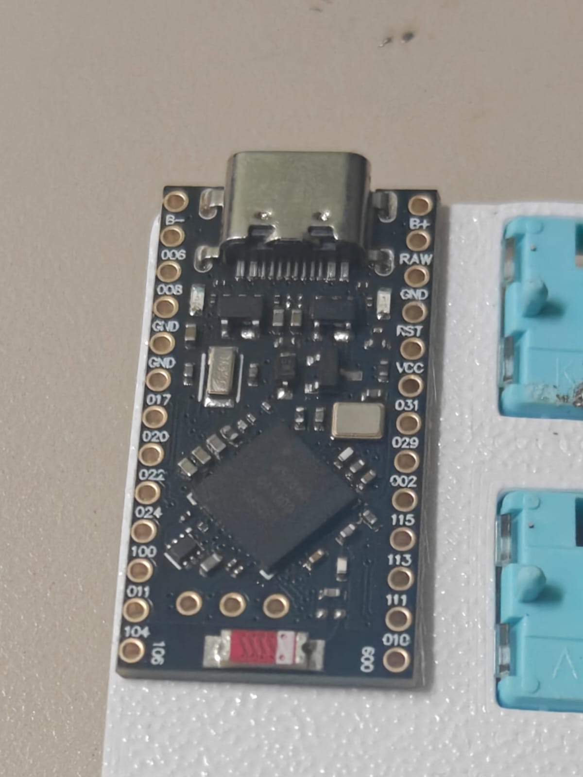 Reading the pin labels on the board itself
I put the four rows on the left edge of the board and the six columns on the right edge, which faces the keys. I skipped two pins that are used for NFC.
Mistake: the row wire on the wrong side of the diode
I soldered the first red lead to the first key. Then it would not beep to the row. I had soldered it to the switch pin, which is on the switch side of the diode. The row is on the stripe side. The diode was doing its job and blocking me.
The fix was simple. The row lead goes on the stripe end of the chain, not on the switch pin.
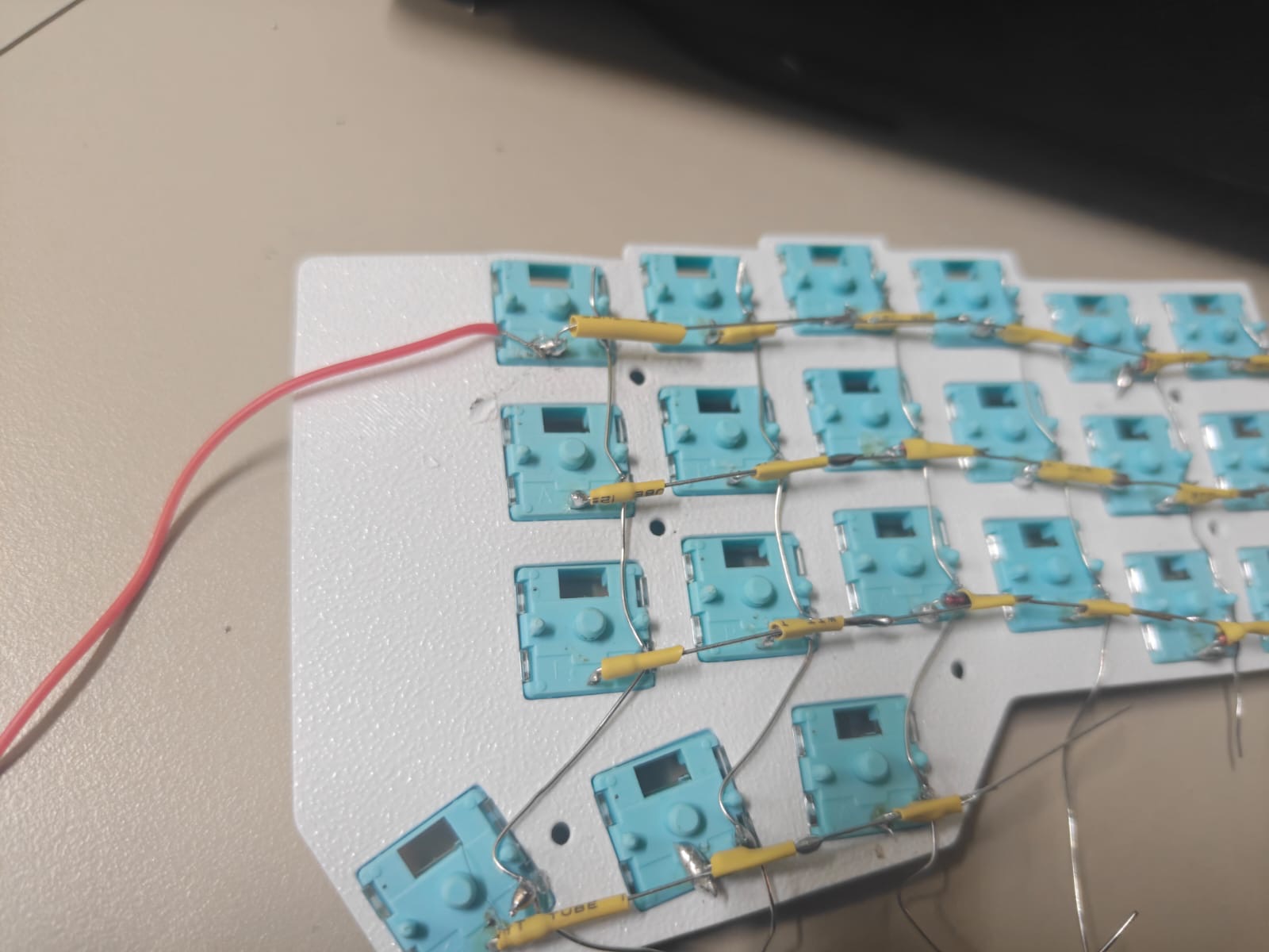 The first board lead. It went on the wrong side of the diode.
With all ten leads on, I soldered them to the board and beep-tested each one. Each row beeped only to its own pin. No row beeped to another row.
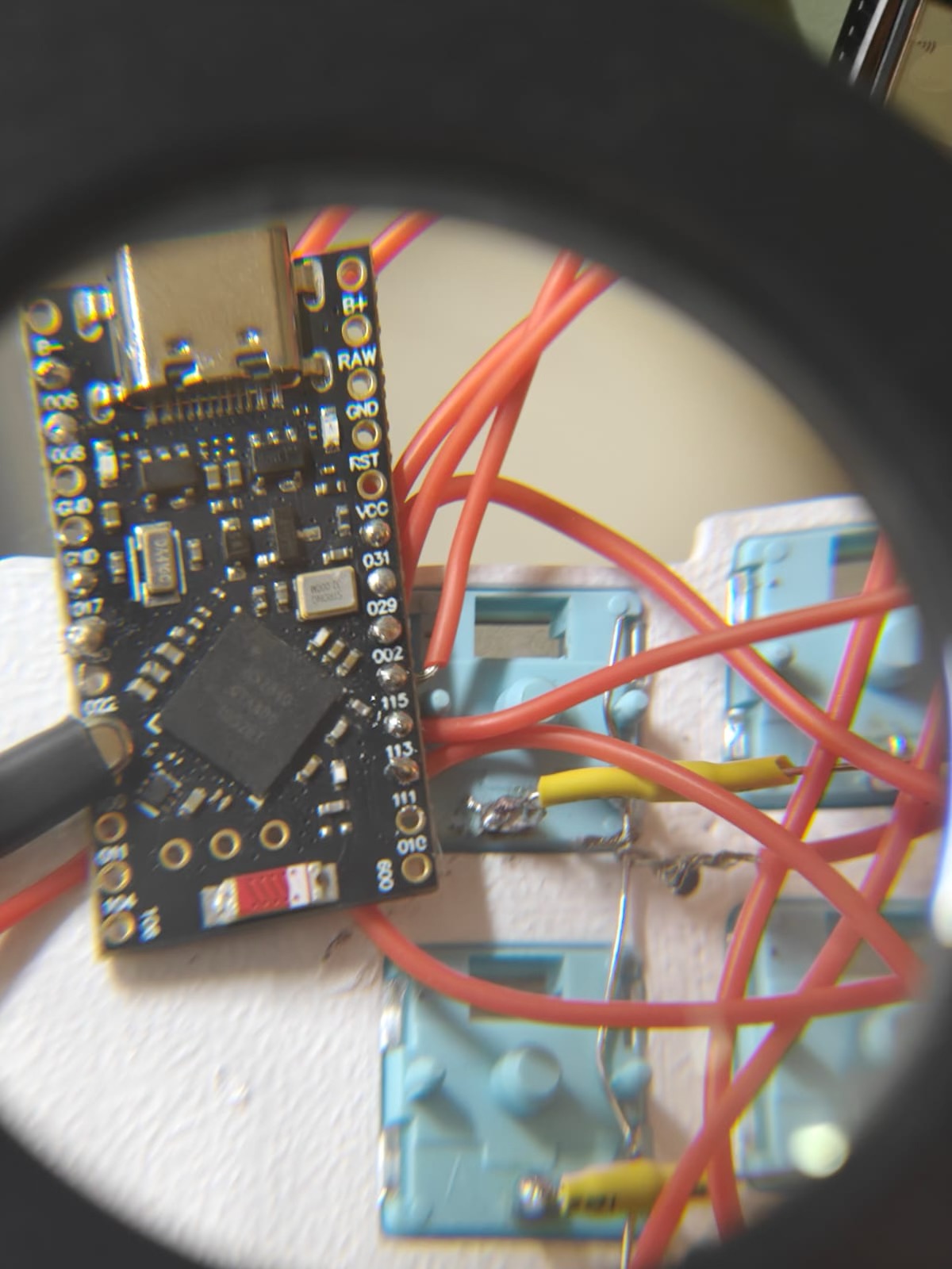 The board wired up. Ten red leads, four rows and six columns.
Firmware with ZMK
ZMK is open-source firmware for wireless keyboards. On a split keyboard, the right half sends its key presses to the left half over Bluetooth. The left half talks to the computer.
You don't need to install a build setup on your laptop. You keep a ZMK config on GitHub, and GitHub Actions builds the firmware files for you. My config tells ZMK three main things:
- The board is a nice!nano.
- The pins for each row and column, in order.
- The diode direction. Mine is "col2row", meaning current flows from column to row.
The keymap is QWERTY with a Lower layer for numbers and arrows, a Raise layer for symbols, and a Bluetooth layer when both are held.
To flash it, I tapped the reset pin to ground twice. The NICENANO drive appeared. I copied the left half's firmware file onto it. The board restarted, and the Mac listed a new USB keyboard.
The first letters
macOS opened its Keyboard Setup Assistant and asked me to press some keys. The first letters I typed were "ac". It worked.
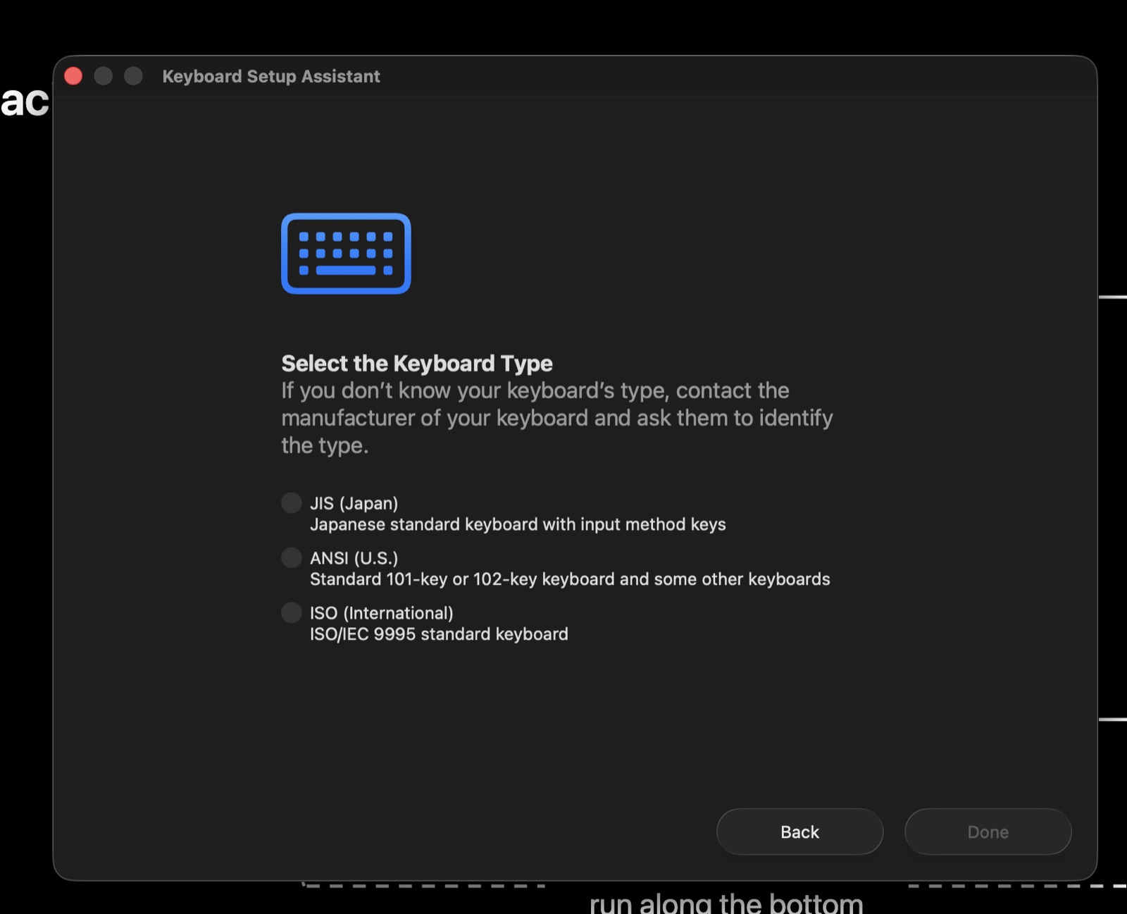 The first thing the keyboard ever typed: "ac", top left
The thumb row that did nothing
I tested every key on a small web page that lights up each key you press. 18 of 20 worked on the first try. The whole thumb row did nothing.
Every link beeped. The thumb row reached its pin. The thumb keys reached their column pins. No shorts. So I blamed the pin. I thought the clone's pad might be dead, and moved the thumb row lead to a different pin. Space started working, so I was sure I had found it.
I hadn't. The real cause was in the firmware. I had soldered the six column leads to the board in the reverse order from my plan. The top row typed T R E W Q from left to right instead of Q W E R T. The thumb keys landed on columns that the firmware ignores for the thumb row.
The fix was one line in the config: reverse the column order. No soldering. Moving the thumb pin had not been needed at all.
The lesson I took: if every wire beeps but a key does nothing, check the firmware pin order before you blame the hardware. Press a whole row and see what letters come out. The order tells you a lot.
By about 10 PM all 21 keys worked, including the Lower key. Hold Lower and press Q, and it types 1.
The case: three tries, no win yet
This is the part that did not work.
Too shallow
The original case had no room for the 45 mm battery. It needed about 3 mm more depth. The slide switch slot was too small too. I made a new version, 3 mm deeper inside with a thicker floor, a bigger USB hole and a proper pocket for the switch. It printed fine.
But the board leads I had left were long, and they made a mess inside.
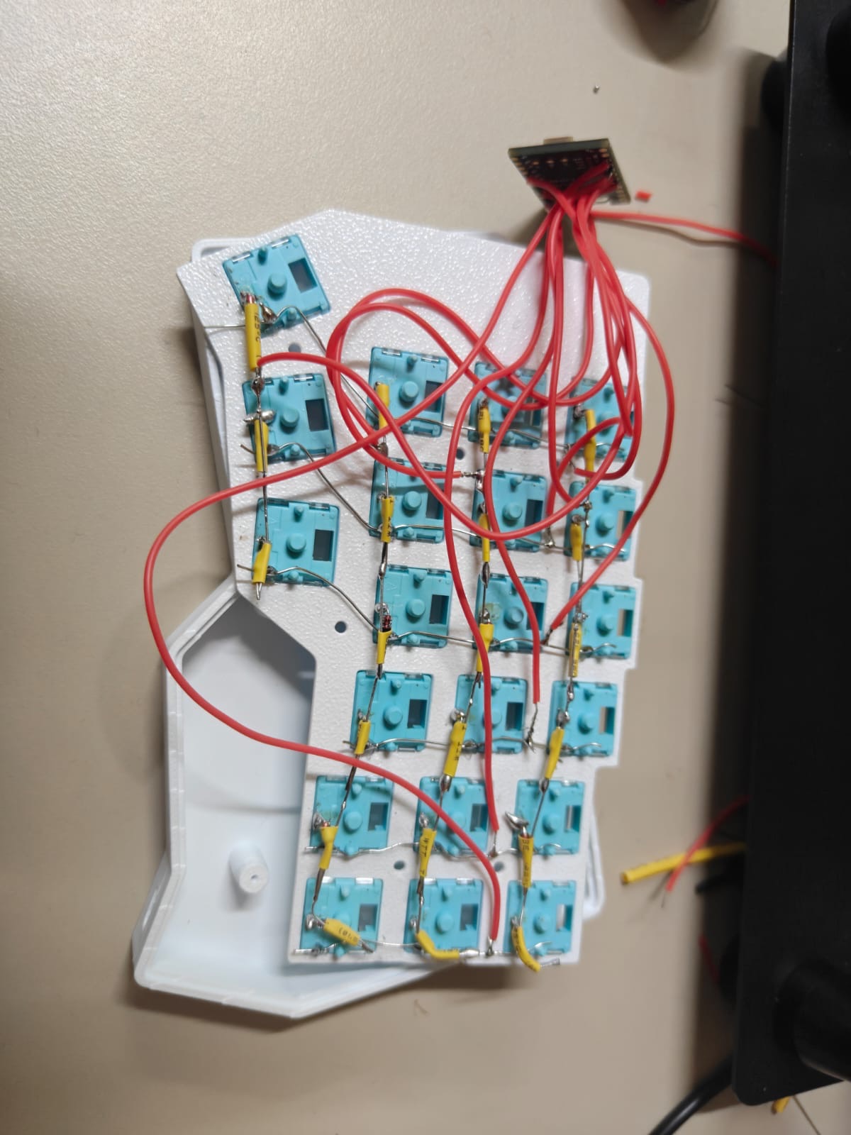 The new case printed, with the plate set on top. The wires are far too long.
Screws that would not go in
The screw holes in the posts were 1.5 mm. They were too tight for M2 screws.
So I tried brass heat-set inserts. You melt them into the plastic with the soldering iron. The first one went in fine. In the next post, melted plastic flowed up into the insert's thread and filled it. The hole had no room below the insert for the pushed plastic to go.
I also found that the plate's screw holes sat 0.77 mm off the post centres. That probably made the screws worse.
I designed two fixes. One is a case that holds the plate with six snap-fit hooks and no screws at all. The other has deeper insert holes with room for the plastic. I also designed small test pieces for each, so I can check the fit in a few minutes before printing a whole case. None of these are tested yet.
A holder built on guesses
The case had a USB hole, but nothing to hold the board in place. I designed a small holder to glue to the floor. I designed it from guessed board sizes instead of measuring. It did not fit the board, and it did not line up with the USB hole.
That one is fully my fault. Measure the real part with calipers before you design around it.
Next: the board on top
Instead of hiding the board under the plate, I want to put it on top, in the empty corner next to the inner column. The wires pass through a slot in the plate. I tried this by melting a slot with the soldering iron, and it already looks cleaner.
It also removes most of my case problems. No holder to guess. Shorter wires. And the case can be much slimmer, because only the battery sits underneath.
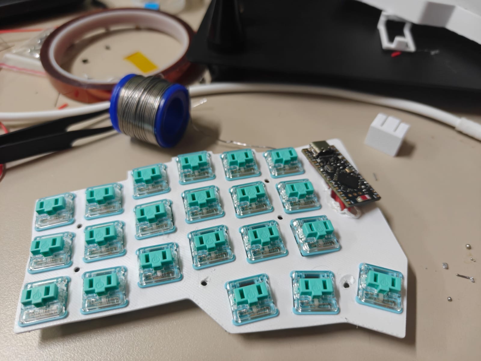 The board on top of the plate, in the empty corner
Next I will design a plate with a pocket for the board, a slot for the wires and a small cover. Then the battery, Bluetooth, and the right half.
Next: part 2, the case and the board on top.